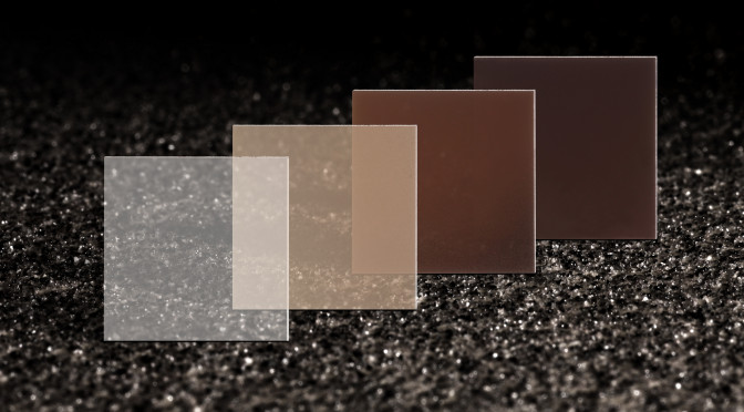
Applied Diamond now offers nitrogen and boron doped diamond materials in both single crystal and polycrystalline products. Making these custom materials available is important in a number of industrial and research areas.
Nitrogen-doped diamond films have been useful as photoluminescence screens for high energy x-ray beam detection and position monitoring. Tailoring the nitrogen level is helpful when finding the optimal image resolution for imaging camera and beam size and path considerations.
At low levels, boron-doped diamond acts as a semiconductor while at high levels it acts as a semimetal giving rise to a number of applications as an electrode. B-doped diamond provides a wide potential window (>3.5V) and low background for higher sensitivity and lower detection limits in bioelectrochemical and electroanalytical applications. Diamond’s biocompatibility and inertness means reduced fouling and ability to withstand extremely corrosive and high temperature/pressure environments as found in water treatment and electrosynthesis work.
Wide band gap semiconductors have properties particularly suited to managing high voltages and frequencies in harsh environments. While SiC, GaN and diamond are all expected to supplant silicon, diamond has the physical and electronic properties most suitable to power electronics. N-type doping is still relatively difficult due to the lack of an efficient donor but p-type doping works well with boron as an acceptor impurity. While results for unipolar devices with coplanar structures have been encouraging, high currents (>100A) though these devices have high on-state resistance. Vertical configurations with ohmic and Schottky contacts on each side are a possible solution but thick >100um freestanding layers, free of defects with metallic-level doping are needed.
Boron-doped diamond has also been found to be superconducting at very low temperatures with a Tc depending upon boron concentration.

